Common voltage levels of digital circuits and basic level shifting required to drive lower voltage devices
When interfacing various devices to a microcontroller, some kind of voltage conversion is often needed. The most common voltage levels of development boards and modules are 3.3 V and 5 V, yet it is not out of the ordinary to find devices using 2.5 V or even 1.8 V I/O levels. This post will explore some of the available methods of converting I/O voltage levels to ensure compatibility between electronic modules and ICs. When I say compatibility I mean the devices connected together through a level shifter should work as expected and not cause damage to each other.
I began searching information about level shifting after a failed attempt to interface an ESP8266 board (3.3 V I/O) to an array of 74HC595-74HC165 shift registers which were required to be powered at 5 V (therefore they expect 5 V I/O). Without documenting too much, I considered 74HC would recognize high 3.3 V output from microcontroller. But that was not the case as I would soon discover. The next step was to add a MOSFET bidirectional level shifter (the ones which are commonly used for I2C), however strange behavior occurred.
What is level shifting?
In this post I will refer to level shifting as the process of converting the logic "1" voltage of a digital I/O to different voltage levels. We are assuming the need to interface two devices which share the same ground, but output different digital voltage levels. This logic "1" level, also known as logic high, is closer to the supply voltage of a device, while the logic "0" (low) level is closer to ground.
Is level shifting really needed for my application?
Only the datasheet of the integrated circuits you are trying to interface can give a proper answer. The useful information can be found in the electrical specifications section. Look for typical power supply voltage (VCC) and input voltage levels which are described as VIL (low input voltage) and VIH (high input voltage). With modern digital ICs, output pin voltages are usually very close to 0 V (when low) or VCC (when high).
But what about input pins? Always remember to check the datasheet to determine if the voltages provided at any input pin can be correctly recognized as low or high level.
- Look at maximum value of VIL. This is usually 0.25...0.3 x VCC. Any level higher than this will not be properly recognized as low. For a reliable design, make sure low signal levels are as close as possible to 0 V.
- Look at minimum value of VIH. This is usually 0.7...0.75 x VCC. Any level lower than this will not be properly recognized as high. For a reliable design, make sure low signal levels are as close as possible to VCC.
But what happens with levels between 0.3...0.7 x VCC? These will certainly cause erroneous, unpredictable behavior, depending on hardly controllable factors such as temperature and signal noise. So, all of the modern ICs have similar high/low voltage limits? Well, most of them, but not all.
TTL vs. CMOS
TTL stands for transistor-transistor logic and it signifies that the signal applied to an input pin is fed to a bipolar transistor (usually to the emitter). The outputs of TTL devices are taken from the collector of a bipolar transistor, which may or may not have a resistor. What is important here is that TTL input pins are current-sinking and they draw current to maintain logic state (and that is not a small current at all - a few milliamps, but sum that up taking into consideration numerous I/O lines of modern electronics). However their advantage is this:
- A low TTL signal is usually between 0 V and 0.8 V.
- A high TTL signal is usually between 2 V and VCC which, by the way, is usually 5 V.
Therefore, a TTL IC can recognize as high a signal between 2 to 5 V. But what about its output? The low output is usually closer to 0 V (0.3...0.5 V), however the high output is far from VCC (given the fact that some of TTL devices used totem-pole outputs). A datasheet for the old 74LS00 NAND gate shows us output high level is typically 3.4 V, yet it could go down to 2.7 V.
Due to their high current demand (even when doing nothing) and low speed, true TTL devices with bipolar transistors do not have very much uses in modern electronics. Another disadvantage is the fixed supply voltage of 5 V (there are also LVTTL devices, suitable for 3.3 V). However, as we will see later, nowadays there are CMOS ICs with TTL compatible inputs.
CMOS stands for complementary metal-oxide-semiconductor, and unlike TTL, it uses pairs of p-type and n-type MOSFETs for logic functions, instead of bipolar transistors. CMOS voltage levels are usually the ones I shown above (VIL < 0.3 x VCC and VIH > 0.7 x VCC). This technology is preferred nowadays because of the fast speed, low current demand (current is required only to change state) and wide range of supply voltage (VCC usually 2 to 6 V). Their disadvantages are the higher sensitivity to electrostatic discharges and low current capability of output pins. Yet, it is the low power requirement of this technology which allowed the miniaturization we see today, with million to billion transistors in a small package.
To answer the first question, with practical examples:
- CMOS output can drive CMOS input only at the same VCC.
- CMOS output can drive TTL compatible input of a device powered from a higher voltage.
- 5 V CMOS output will drive CMOS/TTL inputs of a device powered from 3.3 V, but check the datasheet to see if the I/O pins of the second device are 5 V tolerant! Otherwise, use a level shifter to avoid damage to this device.
- 3.3 V CMOS output cannot directly drive CMOS inputs of a device powered at 5 V. Level shifting is required.
Types of level shifting
Keeping in mind that most I/O ports nowadays are CMOS, while only some have TTL compatible inputs, let's see what kinds of level shifting an application can require. In short, we can have to do the following conversions:
- Unidirectional shifting
- Higher voltage to lower voltage shifting (HV-LV)
- Lower voltage to higher voltage shifting (LV-HV)
- Bidirectional shifting
Of course, one must take into account the number of I/O lines which need to be shifted, if a line will change from input to output and also the speed of the signals.
Voltage divider shifting
Obviously this is the most simple shifting technique. It is limited to unidirectional HV-LV conversion and one must take into account the LV input load, which can drop the voltage output below minimum VIH. This method is useful when a 5 V microcontroller outputs data to a 3.3 V peripheral.
 |
| Voltage divider used as level converter |
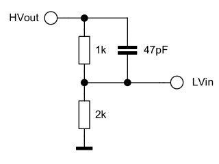
Above is just an example with 1 k and 2 k resistors, which can convert 5 V output to 3.3 V. When choosing resistor values, one must take into account the curent source capabilities of the output pin. In my example, 5 / (1000 + 2000) = 1.66 mA, which is reasonably low for most microcontrollers. But this is not all. You must take into account the input impedance of low voltage pin and make sure it does not cause a significant voltage drop on the divider. I decided to test this circuit, so I used my signal generator to produce a CMOS signal of 5 V amplitude. I fed this signal through the voltage divider to one of the inputs of a buffer gate of 74HC125.
 |
| Testing the voltage divider level shifter |
The red probe on the top is from the signal generator, feeding the CMOS square wave to the 1 k resistor. There is also an oscilloscope probe on the same breadboard line. The second oscilloscope probe is connected to the output of the voltage divider. All other inputs of the IC are grounded, except the one I'm using. I opted to feed the signal to a real CMOS circuit in order to simulate a real usage scenario. At only 100 kHz, this is how the converted signal looks.
 |
| High voltage square wave signal vs. down-shifted with voltage divider at 100 kHz |
Pushing it a little further I get this, at 1 MHz, which no longer looks like a square wave anymore.
 |
| High voltage square wave signal vs. down-shifted with voltage divider at 1 MHz |
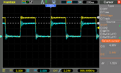
The yellow trace is the signal from generator, 5 V CMOS square wave, while the cyan trace is signal at voltage divider output. At 1 MHz, the gate input capacitance becomes important, the signal looking a little better if I disconnect it from 74HC125. Other than gate capacitance, there are parasitic capacitances which distort the signal, especially on the breadboard.
 |
| Adding a capacitor can counteract the parasitic capacitances |
In my example, to reduce signal distortion I can add a capacitor in parallel with the 1 k resistor, but that would require tuning for a specific frequency. Another alternative, if the output pin can deliver enough current, resistor values can be decreased. This is how the signal looks with the capacitor attached:
 |
| Square wave signal corrected with a capacitor |
In conclusion, resistor divider level shifters can be used with low speed signals, when unidirectional high to low voltage conversion is required. This type of circuit is suitable for CMOS inputs. Do not use it to fed clock signals to devices which react on the rising edge of the clock. Let's design something for higher speeds.
Zener clamping
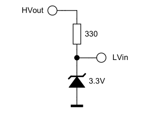
Instead of using a resistive voltage divider, we can clamp the voltage using a Zener diode. The diode junction has a very small capacitance, but it does not affect the signal too much. The circuit looks as follows, however there are some things to consider.
 |
| Voltage clamping with Zener diode |
Below 5.6 V, the Zener effect is predominant in these diodes. Their breakdown voltage varies with temperature, yet the variation shouldn't cause any problems in this application. Another issue is that, in order to maintain the diode in reverse breakdown, a minimum current is required (of a few mA).
Therefore the series resistor value must be decreased and the output pin must drive a bigger load. For example, BZX79C3V3 requires at least 5 mA. In the above circuit, (5 - 3.3)/0.005 = 340 ohms is the maximum value the resistor can be. What is the minimum value? For this, one must take into account the Zener power dissipation and available current on output pin.
 |
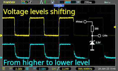
| Voltage shifting with Zener clamp |
It is obvious that the signal still looks good even at high(er) frequencies. Keep in mind that the test is made on a breadboard.
In conclusion, Zener clamp shifters may be used with higher speed signals as long as the output pins can provide enough current to keep the diode in reverse breakdown.
Overview
This post got long enough, so I will continue the topic of level shifting in one or more follow-up posts. This time I showed you two simple passive methods of reducing the voltage of a signal, which can be used as unidirectional higher-to-lower level shifters. I would only recommend these methods for low speed signals, such as chip enable and some interrupt requests. I wouldn't use such converters for clock and serial data. Next time we will explore active converters, made with discrete components or available as integrated circuits.
References
- Wikipedia contributors. "Transistor–transistor logic." Wikipedia, The Free Encyclopedia, 19 Jan. 2023. Web. 24 Jan. 2023.
- Wikipedia contributors. "CMOS." Wikipedia, The Free Encyclopedia, 16 Jan. 2023. Web. 24 Jan. 2023.
- Fairchild. DM74LS00 datasheet on Futurlec.
- Diodes Inc. 74HC00 datasheet.
- Wikipedia contributors. "Zener diode." Wikipedia, The Free Encyclopedia, 15 Dec. 2022. Web. 25 Jan. 2023.


No comments :
Post a Comment
Please read the comments policy before publishing your comment.