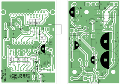
How to generate PCB artwork from KiCAD projects. Silkscreen with PCB layer see through that is suitable for displaying on screen
KiCAD is probably the most complete opensource EDA suite. It comes with a schematic editor, a PCB designer and a 3D viewer. PCB designs can be exported to multiple formats or printed directly from the software. Although the plotting (printing) options are quite advanced, there aren't options for overlaying different layers with different colors.
This tutorial will show you how to create PCB artwork that looks good on display or print and that is intended only as a guide to the reader, not as a source for manufacturing PCB. The result will be a greenish PCB (or any color you want) with silkscreen on top of it. This is probably something you already seen in electronics publications.
There are many ways of doing this. All you need to start are the PDF files plotted by KiCAD and some image editing software (I prefer opensource tools: GIMP or some ImageMagick scripting).

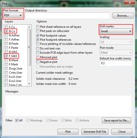
To start, open a finished PCB design in KiCAD and plot some layers. Go to File - Plot and make sure format is set to PDF. You must select a copper layer and a silkscreen. For example, in most situations you will want to plot the bottom copper layer (B.Cu) with the top silkscreen (F.SilkS). If your PCB is SMT build mostly on top copper layer, you will want F.Cu with F.SilkS. On the other hand, if your PCB is built on bottom layer with SMD parts, you will make a mirrored plot of B.Cu and B.SilkS. You should also plot some drill marks. I prefer small marks.

KiCAD plotting options
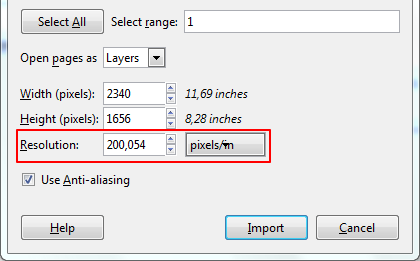
The result of the plot will be two files: a copper layer and a silkscreen plot. Next, I will import these in GIMP. Launch GIMP and first load the copper layer PDF file. It will ask for some parameters. Select the first (and only) page and set a resolution of 200 DPI (or more). Now load the second PDF (silkscreen) as layer in GIMP (File - Open as Layers or drag and drop and select Open pages as: Layers). Make sure you set the exact same resolution as you did with the other PDF!

Import PDF in GIMP
You should now have a GIMP image with two layers and you currently see only silkscreen. You can go ahead and perform and automatic crop (Image - Autocrop Image). This will remove the unnecessary white margins.
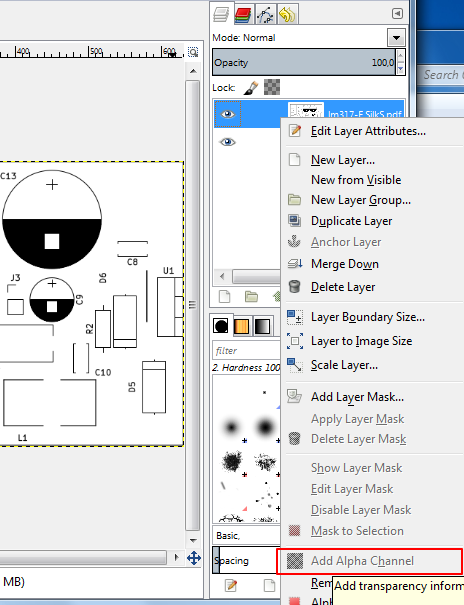
The first problem is that silkscreen layer is not transparent. Right click this layer and try to Add alpha channel. If it's disabled, then the layer already has an alpha channel.

Add alpha channel to layer in GIMP
With this layer selected, go to Colors - Color to alpha and make sure From color is white. Click OK. The silkscreen layer is now transparent.

GIMP color to alpha
Now select the copper layer and go to Colors - Colorize. This is the point where you try different values until you get what you like.

Colorize copper layer in GIMP
Once you're done, go to File and Export image to PNG. That's it.
All this is also doable using ImageMagick. And here comes the advantage of command line tools: scripting. The steps can be summarized as follows:
- Convert plotted PDFs to PNG (Ghostscript needed);
- Take copper layer PNG and colorize it;
- Take silkscreen layer PNG and make it transparent;
- Overlay the PNGs in the correct order;
- Auto-crop resulted image.
For this I made a small shell script that takes the KiCAD project directory as input parameter and generates the PNG file. The script currently has some issues, but if you want to try it you can find it on GitHub.


Thank you for posting this, it is the first time I've come across an article dealing with KiCAD artwork that led to some semblance of success on my part. I used it to export edge layers, then editing artwork within those boundaries and imported it in again (with the same DPI) setting as silkscreen artwork - only change was that I couldn't have transparency in the image for it to work.
ReplyDeleteThank you for the feedback. The method is not quite straightforward, but it has some possible uses.
Delete