Buffered (E)JTAG adapter with schematic and PCB design. Parallel port interface.
JTAG is an in-circuit programming and debugging interface. It specifies the use of a dedicated debug port implementing a serial communications interface for low-overhead access without requiring direct external access to the system address and data buses. The interface connects to an on-chip test access port (TAP) that implements a stateful protocol to access a set of test registers that present chip logic levels and device capabilities of various parts.
JTAG interface is supported by many devices as a convenient way of rewriting firmware (specially boot loaders) when other methods fail. Using JTAG, the ROM memory can be directly written without desoldering it from PCB to program it using a specific programmer.
In most cases, you will need JTAG access to a device with a no longer working bootloader. Otherwise, if the bootloader runs, there should be easier ways of debricking the deice. Most of the times, a device with corrupt bootloader will not display any signs of working (i.e. no LEDs turned on in case of routers, no display on front panel of set-top-boxes). Nor any ports of the device will work (i.e. no serial port response, no network detected).

There are a lot of different JTAG connectors you can find on devices. If you are lucky, the JTAG port will be populated with a pinheader so you can connect to it. There is also the case of a non populated PCB footprint and the worst, no JTAG port at all - the only way being to solder directly to CPU pins (that if you know which ones).
There are two main types of JTAG adapters you can build. Both of them connect to the parallel (LPT) port of the computer and work with software that bit-bangs JTAG protocol to LPT pins. Modern computers do not come with a motherboard LPT port, so you will need an USB adapter (note that it may not work) or PCI expansion card. The easiest to build is the unbuffered type of cable. You just use some current limiting resistors between the LPT port and JTAG port. This is not quite recommended because LPT uses 5 V levels and your device may be using a different voltage (2.5 V or 3.3 V). The device might get damaged or the interface will repeatedly throw communication errors. An unbuffered cable is good for a SoC operating at 5 V.
Buffered adapter is a better alternative, although it is a bit harder to build because it requires more parts. Its main advantage is that the voltage levels match those expected by the device. More than that, some JTAG ports provide a voltage reference that can be used to power the adapter and provide the same voltage levels through the signal pins. Below is the schematic of a buffered JTAG adapter.

Buffered JTAG schematic
The adapter uses only one integrated circuit (the 74HC244 line driver) and some common parts. P2 pinheader controls power source. If you place a jumper on pins 1 and 2, power must be supplied by the target device through JTAG port (You can see if target device supplie power via JTAG port if D4 LED turns on). Otherwise, place a jumper across pin 2 and 3 and supply DC voltage to the adapter. P1 pinheader allows nSRST to be pulled-up to supply voltage (using a jumper) if the CPU does not support open collector output. This is needed by some MIPS chipsets that make use of EJTAG protocol. P3 pinheader is the JTAG port. You will have to build different cables that will connect it to the port of each device. P4 pinheader changes port voltage (it has effect only if external supply is used).
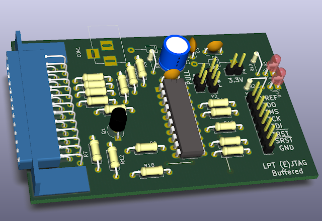
The adapter can be built on a single sided 80 x 55 mm printed circuit board. All parts are through hole devices except the voltage regulator which is SMD. Don't forget about it.

SMD Voltage regulator
The current configuration allows 3.3 V and 5 V signal levels. By using a 2.5 V regulator you can have this level if you need. Zener dioded D2 can be replaced with two series 1N4001 fitted in reverse order, to achieve a voltage drop of about 1.4 V that will raise output of voltage regulator to 4.7 V. If you use a 2.5 V regulator, you can raise its output to 3.3 V with a single 1N4001 fitted in reverse (2.5 + 0.7 = 3.2 V) or if you need 5 V level you can use 2.7 V Zener diode. You can't use a regulator with less that 2 V output because this is the minimum voltage supported by 74HC244.

PCB layout
You should connect to computer with target device unpowered. If when powering the device, LED D4 INT.PWR turns on, you don't need to use an external power supply. Just make sure there is a jumper between pins 1 and 2 of connector P2. Otherwise, you must power the adapter with a DC voltage of about 8 - 16 V via CON1 and place the jumper on pins 2 and 3 of header P2. LED D3 EXT.PWR will turn on.
To be able to perform JTAG operations you must connect using a computer software. There are a lot of options here. Although it was last updated in 2009, for me UrJTAG worked. It is open source and supports unbuffered cables (EA253, DLC5) but also buffered adapters like this one (Wiggler, Wiggler2).

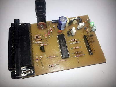
Built Wiggler JTAG buffered adapter
Downloads
References
- Wikipedia contributors. "JTAG," Wikipedia, The Free Encyclopedia, https://en.wikipedia.org/w/index.php?title=JTAG&oldid=765818413 (accessed February 18, 2017).
- XJTAG Limited. What is JTAG and how can I make use of it? https://www.xjtag.com/about-jtag/what-is-jtag/ (accessed February 18, 2017).
- Peter Green. Answer on What is a JTAG? on Electrical Engineering StackExchange.
- OpenWrt Wiki. Buffered Cable, Wiggler. https://wiki.openwrt.org/doc/hardware/port.jtag.cable.buffered (accessed February 18, 2017).
- DO999. How to build “Megavolt’s Small Buffered JTAG v1.2” http://www.angelfire.com/ex2/spider9909/New%20files/bjtag101.pdf (accessed February 18, 2017).
- MIPS Technologies Inc. EJTAG Specification. http://downloads.buffalo.nas-central.org/LS2_MIPSel/DevelopmentTools/JTAG/MD00047-2B-EJTAG-SPC-03.10.pdf (accessed February 18, 2017).


No comments :
Post a Comment
Please read the comments policy before publishing your comment.