How to make your circuit boards using the free PCB design software ExpressPCB.
In the previous tutorials we
simulated a circuit idea and turned it into a
schematic. Now it is time to make a PCB design. I have chosen for this the free PCB design software from
ExpressPCB. They also offer ExpressSCH, a schematic capture software which is quite good but doesn't have powerful drawing capabilities. This software is available only for Windows operating system but it runs in Linux too using Wine.
ExpressPCB is very easy to use and one of the features I like most is that it is very easy to make new footprints. You don't even need to leave the current PCB design window. You just draw the footprint using predefined pads and shapes then group all elements into a component footprint. That is all. If you want this to be available in other projects, you just add it to library.
There are also some downsides. The export dialog is quite limited and you can't directly export mirrored layouts. However there is a workaround that I will show you.
We started to design a dark activated switch for which we now have a schematic. In order to make the PCB we need pinout and footprint information for some of the parts: the opamp and the relay. While the opamp uses a standard DIP-8 capsule that we can find in the library, for the relay I will draw the footprint according to the datasheet.
 |
| G2RL footprint |
Let's start ExpressPCB now and add the pads. First of all we will set a grid of 0.5 mm that is suitable for this footprint. From
View menu choose
Options. Set Units to
mm and snapping to
.5.
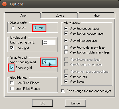 |
| Setting the grid units and snapping |
After adding the pads and drawing the silkscreen, drag with the mouse to select the footprint and group it into a component.
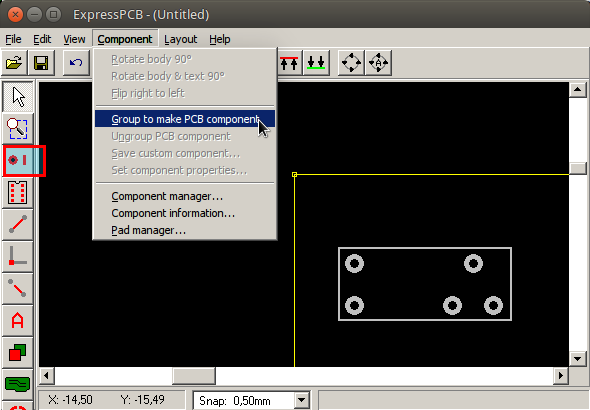 |
| Making PCB component |
If you want to add this new component to the custom libraries, just click to select it and from the same
Component menu choose
Save custom component. A dialog will appear prompting you to enter a name for the footprint.
We can add all the remaining components to the project now. For the LDR we will use a simple two pin connector footprint or even a 5 mm LED footprint works. I recommend switching back to the default grid of 0.050".
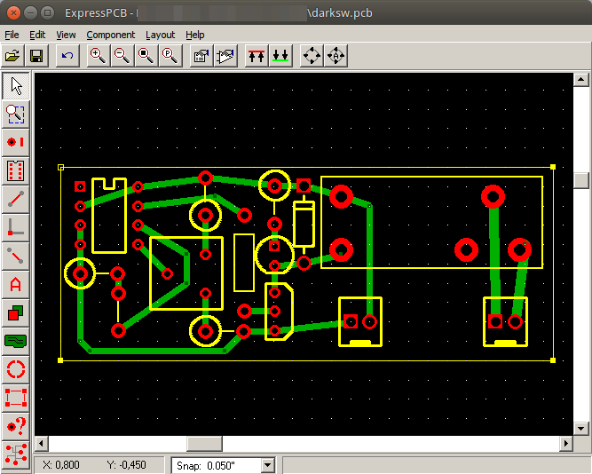 |
| Finished project in ExpressPCB |
ExpressPCB is easy to use. Select the tool you want from the left vertical toolbar and specific options will appear on the top horizontal toolbar. You can resize the PCB only from three corners (not the top left one). We can now complete the design by adding some component references or values on the silkscreen layer.
Now let's see how we can export this project. There are only two options in the File menu. One for DXF output and the other with bitmap output. This is what the bitmap renders.
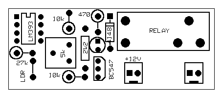 |
| ExpressPCB bitmap |
There are no other options to change so we'll look further at the
Print dialog. Neither here is a mirror option, so the remaining alternative is to print to a virtual PDF printer, then import the result in an image editor and flip the image while preserving physical size and DPI information.
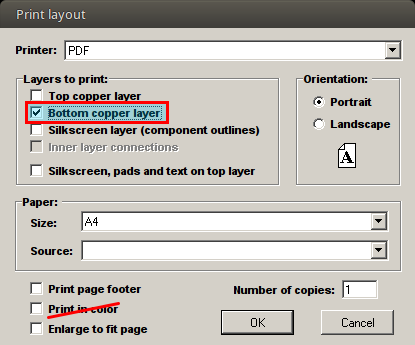 |
| ExpressPCB print dialog |
The result looks good and if you don't need a mirrored PCB image, you can print directly. Otherwise, print to PDF and open the image with GIMP. I recommend a resolution of 600 DPI without antialiasing. Then you can flip the image and save it. I recommend saving to TIFF format because it handles DPI metadata. Afterwards you can print image at real size or embed it into a document using LibreOffice Draw (for example).
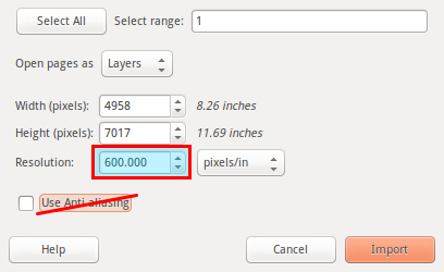 |
| Importing PCB into GIMP |
Here is an example of what you can obtain if you import different images into LibreOffice Draw. The physical size is preserved.
Have you ever used ExpressPCB? I forgot to mention it features a PCB manufacturing service and you can order PCBs directly from it.


This EDA Express PCB Design overview is insightful. When tackling intricate projects, leveraging specialized PCB Design Services can elevate your results. These services bring expertise in layout, routing, and manufacturability, ensuring a polished design that meets the highest standards. A definite asset for achieving top-notch PCB outcomes.
ReplyDelete